- 您现在的位置:买卖IC网 > Sheet目录2001 > ISL35822LPIK (Intersil)IC CLOCK/DATA RECOVERY 192EBGA-B
32
Note (1): These 1-byte register values are merely copied by the ISL35822 from the I2C address space on Power-up or RESET, or on a periodic or on-demand direct
DOM update operation (i.e. with Register bit 1.C018’h.2 Table 51 not set) under the control of Register 1.A100’h (Table 38). The ISL35822 takes no action as
a result of the values copied.
Note (1): These 1-byte register values are copied by the ISL35822 from the I2C address space on Power-up or RESET, or on any DOM read operation. If the ‘Indirect
DOM Enable’ bit (Register bit 1.C018’h.2 Table 51) is not set, a four-lane external DOM device is expected to determine the values for these registers,
according to Section 11.3 in the XENPAK MSA Rev 3.0 specification. A single one-lane DOM device system will provide the values from the single DOM
device here. If the ‘Indirect DOM Enable’ bit is set, the values from the “Representative” (as set by Register bits 1.C018’h.1:0 in Table 51) lane DOM are
entered here. See “DOM Registers” on page 16. These bits are gated with the enable bits in 1.9006:7 (Table 30 & Table 31) and the LX4/CX4 select
LX4_MODE pin to drive bits 1.9004.1 & 1.9003.1 (Table 28 & Table 27), and if enabled via 1.9002 & 1.9001 (Table 25 & Table 24) to drive the LASI pin.
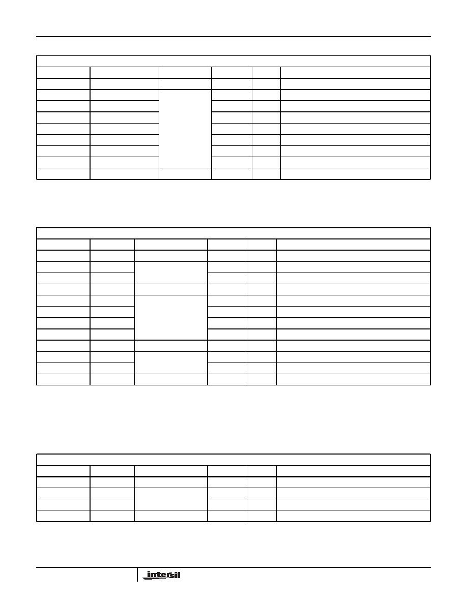
Table 35. XENPAK DOM EXTENDED CAPABILITY REGISTER
MDIO REGISTER, ADDRESS = 1.41071 (1.A06F’h)
BIT
NAME
SETTING
DEFAULT
R/W
DESCRIPTION(1)
1.41071.15:8
Reserved
00’h(1)
1.41071.7
TT_Able
1 = Indicates
Capability
Implemented
0 = Not
Implemented
RO
Transceiver Temp Monitoring Capable
1.41071.6
LBC_Able
RO
Laser Bias Current Monitoring Capable
1.41071.5
LOP_Able
RO
Laser Output Power Monitoring Capable
1.41071.4
ROP_Able
RO
Receive Optical Power Monitoring Capable
1.41071.3
AL_Able
RO
Alarm Flags for Monitored Quantities
1.41071.2
WN_Able
RO
Warning Flags for Monitored Quantities
1.41071.1
MON_LASI
RO
Monitoring Quantities Input to LASI
1.41071.0
Reserved
RO
Monitoring Capable
Table 36. XENPAK DOM ALARM FLAGS REGISTER
MDIO REGISTER, ADDRESS = 1.41072:3 (1.A070:1’h)
BIT
NAME
SETTING
DEFAULT
R/W
DESCRIPTION(1)
1.41072.15:8
Reserved
00’h(1)
RO
1.41072.7
TT_High
1 = Alarm Set
0 = Alarm Not Set
0’b
RO
Transceiver Temp High Alarm
1.41072.6
TT_Low
0’b
RO
Transceiver Temp Low Alarm
1.41072.5:4
Reserved
00’b
1.41072.3
LBC_High
1 = Alarm Set
0 = Alarm Not Set
0’b
RO
Laser Bias Current High Alarm
1.41072.2
LBC_Low
0’b
RO
Laser Bias Current Low Alarm
1.41072.1
LOP_High
0’b
RO
Laser Output Power High Alarm
1.41072.0
LOP_Low
0’b
RO
Laser Output Power Low Alarm
1.41073.15:8
Reserved
00’h
1.41073.7
ROP_High
1 = Alarm Set
0 = Alarm Not Set
0’b
RO
Receive Optical Power High Alarm
1.41073.6
ROP_Low
0’b
RO
Receive Optical Power Low Alarm
1.41073.5:0
Reserved
00’h
Table 37. XENPAK DOM WARNING FLAGS REGISTER
MDIO REGISTER, ADDRESS = 1.41076:7 (1.A074:5’h)
BIT
NAME
SETTING
DEFAULT
R/W
DESCRIPTION(1)
1.41076.15:8
Reserved
00’h(1)
1.41076.7
TT_High
1 = Warning Set
0 = Warn. Not Set
0’b
RO
Transceiver Temp High Warning
1.41076.6
TT_Low
0’b
RO
Transceiver Temp Low Warning
1.41076.5:4
Reserved
00’b
ISL35822
发布紧急采购,3分钟左右您将得到回复。
相关PDF资料
ISL41334IRZ-T7A
IC TXRX RS232/485 DL 2PRT 40QFN
ISL43485IB-T
IC TXRX 1TX/1RX 3V RS-485 8-SOIC
ISL51002CQZ-110
IC FRONT END 10BIT VID 128-MQFP
ISL5314IN
IC SYNTHESIZER DIGITAL 48-MQFP
ISL55100AIRZ-T
IC COMP DRVR/WINDOW 18V 72-QFN
ISL55100BIRZ
IC COMP DRVR/WINDOW 18V 72-QFN
ISL5627INZ
IC DAC DUAL 8BIT 3.3V 48-LQFP
ISL5629/2INZ
IC DAC 8BIT CMOS DUAL 48LQFP
相关代理商/技术参数
ISL36111
制造商:INTERSIL 制造商全称:Intersil Corporation 功能描述:11.1Gb/s Lane Extender
ISL36111DRZ-EVALZ
功能描述:EVAL BOARD FOR ISL36111DRZ RoHS:是 类别:编程器,开发系统 >> 评估演示板和套件 系列:* 产品培训模块:Obsolescence Mitigation Program 标准包装:1 系列:- 主要目的:电源管理,电池充电器 嵌入式:否 已用 IC / 零件:MAX8903A 主要属性:1 芯锂离子电池 次要属性:状态 LED 已供物品:板
ISL36111DRZ-T7
功能描述:IC EQUALIZER REC 11.1GBPS 16QFN RoHS:是 类别:集成电路 (IC) >> 接口 - 专用 系列:QLx™ 特色产品:NXP - I2C Interface 标准包装:1 系列:- 应用:2 通道 I²C 多路复用器 接口:I²C,SM 总线 电源电压:2.3 V ~ 5.5 V 封装/外壳:16-TSSOP(0.173",4.40mm 宽) 供应商设备封装:16-TSSOP 包装:剪切带 (CT) 安装类型:表面贴装 产品目录页面:825 (CN2011-ZH PDF) 其它名称:568-1854-1
ISL36111DRZ-TS
功能描述:IC EQUALIZER REC 11.1GBPS 16QFN RoHS:是 类别:集成电路 (IC) >> 接口 - 专用 系列:QLx™ 标准包装:3,000 系列:- 应用:PDA,便携式音频/视频,智能电话 接口:I²C,2 线串口 电源电压:1.65 V ~ 3.6 V 封装/外壳:24-WQFN 裸露焊盘 供应商设备封装:24-QFN 裸露焊盘(4x4) 包装:带卷 (TR) 安装类型:表面贴装 产品目录页面:1015 (CN2011-ZH PDF) 其它名称:296-25223-2
ISL36356A-APDK
制造商:INTERSIL 制造商全称:Intersil Corporation 功能描述:PRISM 11Mbps Wireless Local Area Network Access Point
ISL36356A-APDK-EVAL
制造商:INTERSIL 制造商全称:Intersil Corporation 功能描述:PRISM 11Mbps Wireless Local Area Network Access Point
ISL36411
制造商:INTERSIL 制造商全称:Intersil Corporation 功能描述:Quad Lane Extender
ISL36411DRZ-EVALZ
功能描述:EVAL BOARD FOR ISL36411DRZ RoHS:是 类别:编程器,开发系统 >> 评估演示板和套件 系列:* 产品培训模块:Obsolescence Mitigation Program 标准包装:1 系列:- 主要目的:电源管理,电池充电器 嵌入式:否 已用 IC / 零件:MAX8903A 主要属性:1 芯锂离子电池 次要属性:状态 LED 已供物品:板